- 您现在的位置:买卖IC网 > Sheet目录1219 > HI5746EVAL1 (Intersil)EVALUATION PLATFORM HI5746
�� �
�
�Application� Note� 9725�
�?ip-?op� and� the� last� two� provide� CLK� and� CLK� at� the� data�
�output� connector,� P2.� The� clock/data� relationship� at� the� P2�
�output� connector� is� as� follows.� CLK� has� rising� edges� aligned�
�with� data� transitions� and� CLK� has� rising� edges� mid-bit.�
�The� data� corresponding� to� a� particular� analog� input� sample� will�
�be� available� at� the� digital� outputs� of� the� HI5746� after� the� data�
�latency� (7� cycles)� plus� the� HI5746� digital� data� output� delay.�
�The� sample� clock� and� digital� output� data� signals� are� buffered�
�and� made� available� through� two� connectors� contained� on� the�
�evaluation� board.� The� line� buffering� allows� for� driving� long� leads�
�see� Figure� 4.� The� performance� of� the� ADC� does� not� change�
�signi?cantly� with� the� value� of� the� analog� input� common�
�mode� voltage.�
�A� DC� voltage� source,� V� DC� ,� equal� to� 3.2V� (typical),� is� made�
�available� to� the� user� to� help� simplify� circuit� design� when� using�
�an� AC� coupled� differential� input.� This� low� output� impedance�
�voltage� source� is� not� designed� to� be� a� reference� but� makes� an�
�excellent� DC� bias� source� and� stays� well� within� the� analog�
�input� common� mode� voltage� range� over� temperature.�
�or� analyzer� inputs.� These� drivers� are� not� necessary� for� the�
�digital� output� data� if� the� load� presented� to� the� converter� does�
�not� exceed� the� data� sheet� CMOS� drive� limits� and� a� load�
�capacitance� of� 10pF.� P1� allows� the� evaluation� board� to� be�
�interfaced� to� the� DSP� evaluation� boards� available� from� Intersil�
�and� should� be� installed� on� the� far� side� (layer� 4)� of� the�
�evaluation� board� for� proper� signal� routing� to� the� DSP� evaluation�
�V� IN�
�-V� IN�
�V� IN� +�
�V� DC�
�V� IN� -�
�HI5746�
�boards.� The� digital� output� data� and� sample� clock� can� also� be�
�accessed� by� clipping� the� test� leads� of� a� logic� analyzer� or� data�
�acquisition� system� onto� the� I/O� pins� of� connector� P2.�
�The� A/D� converters� OE� control� input� pin� allows� the� digital�
�output� data� bus� of� the� converter� to� be� switched� to� a� three-�
�state� high� impedance� mode.� This� feature� enables� the� testing�
�and� debugging� of� systems� which� are� utilizing� one� or� more�
�converters.� This� three-state� control� signal� is� not� intended� for�
�use� as� an� enable/disable� function� on� a� common� data� bus�
�FIGURE� 3.� AC� COUPLED� DIFFERENTIAL� INPUT�
�The� HI5746EVAL1� evaluation� board� accepts� a� single-ended�
�analog� input� and� converts� it� to� a� differential� signal� for� driving�
�the� V� IN� +� and� V� IN� -� analog� inputs� of� the� converter.� The�
�single-ended� to� differential� conversion� is� accomplished�
�through� the� use� of� two� operational� ampli?ers� (U1� and� U2).�
�U1� is� con?gured� as� a� unity� gain� ampli?er� and� U2� is�
�con?gured� as� an� inverting� ampli?er� with� a� gain� of� minus� one.�
�and� could� result� in� possible� bus� contention� issues.� The� A/D�
�converters� OE� control� input� pin� is� controlled� by� the�
�installation� or� removal� of� a� shunt,� JP1,� contained� on� the�
�evaluation� board.� Installation� of� JP1� forces� the� OE� control�
�input� pin� low� for� normal� operation� while� removal� of� JP1�
�allows� the� digital� output� data� bus� of� the� converter� to� be�
�+5V�
�V� IN� +�
�V� IN� +�
�0.5V� P-P�
�0.5V� P-P�
�V� IN� -�
�VDC� =� 4.75V�
�V� IN� -�
�0.25V� <� VDC� <� 4.75V�
�+5V�
�switched� to� a� three-state� high� impedance� mode.�
�Analog� Input�
�The� fully� differential� analog� input� of� the� HI5746� A/D� can� be�
�0V�
�V� IN� +�
�0.5V� P-P�
�V� IN� -�
�VDC� =� 0.25V�
�0V�
�con?gured� in� various� ways� depending� on� the� signal� source�
�and� the� required� level� of� performance.�
�Differential� Analog� Input� Con?guration�
�For� the� AC� coupled� differential� input� (Figure� 3)� assume� the�
�difference� between� V� REF� +,� typically� 2.5V,� and� V� REF� -,� typically�
�2.0V,� is� 0.5V.� Fullscale� is� achieved� when� the� V� IN� and� -V� IN� input�
�signals� are� 0.5V� P-P� ,� with� -V� IN� being� 180� degrees� out� of� phase�
�with� V� IN� .� The� converter� will� be� at� positive� fullscale� when� the�
�V� IN� +� input� is� at� V� DC� +� 0.25V� and� the� V� IN� -� input� is� at� V� DC� -�
�0.25V� (V� IN� +� -� V� IN� -� =� +0.5V).� Conversely,� the� converter� will� be�
�at� negative� fullscale� when� the� V� IN� +� input� is� equal� to� V� DC� -�
�0.25V� and� V� IN� -� is� at� V� DC� +� 0.25V� (V� IN� +� -� V� IN� -� =� -0.5V).�
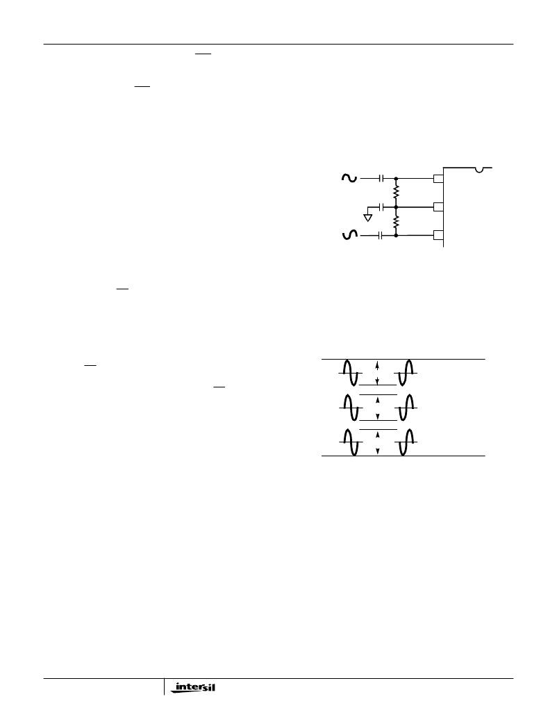
�Since� the� HI5746� is� powered� by� a� single� +5V� analog� supply,�
�the� analog� input� is� limited� to� be� between� ground� and� +5V.�
�For� the� differential� input� connection� this� implies� the� analog�
�input� common� mode� voltage� can� range� from� 0.25V� to� 4.75V,�
�FIGURE� 4.� DIFFERENTIAL� ANALOG� INPUT� COMMON� MODE�
�VOLTAGE� RANGE�
�HI5746� Performance� Characterization�
�Dynamic� testing� is� used� to� evaluate� the� HI5746�
�performance.� Among� these� tests� are� Signal-to-Noise� and�
�Distortion� Ratio� (SINAD),� Signal-to-Noise� Ratio� (SNR),� Total�
�Harmonic� Distortion� (THD),� Spurious� Free� Dynamic� Range�
�(SFDR)� and� InterModulation� Distortion� (IMD).�
�Figure� 5� shows� the� test� system� used� to� perform� dynamic�
�testing� on� high-speed� ADC’s� at� Intersil.� The� clock� (CLK)� and�
�analog� input� (AIN)� signals� are� sourced� from� low� phase� noise�
�HP8662A� synthesized� signal� generators� that� are� phase�
�locked� to� each� other� to� ensure� coherence.� The� output� of� the�
�signal� generator� driving� the� ADC� analog� input� is� bandpass�
�?ltered� to� improve� the� harmonic� distortion� of� the� analog� input�
�signal.� The� comparator� on� the� evaluation� board� will� convert�
�the� sine� wave� CLK� input� signal� to� a� square� wave� to� drive� the�
�3-5�
�发布紧急采购,3分钟左右您将得到回复。
相关PDF资料
HIP1011AEVAL1
EVAL BOARD PCI HOT PLUG HIP1011
HIP1011DEVAL1
EVAL BOARD PCI HOT PLUG DUAL
HIP1011EVAL1
PCI HOT PLUG EVALUATION BOARD
HIP1011EVAL2
EVAL BOARD COMPACT PCI HOT PLUG
HIP1012EVAL1
EVALUATION BOARD DUAL GENERIC
HIP1013EVAL1
EVALUATION BOARD DUAL GENERIC
HIP2100EVAL2
EVAL BOARD 48VDC-5UDC CONVERTER
HIP2100EVAL
EVAL BOARD MINI HALF BRIDGE
相关代理商/技术参数
HI5746KCA
功能描述:IC ADC 10-BIT 40MSPS 28-SSOP RoHS:否 类别:集成电路 (IC) >> 数据采集 - 模数转换器 系列:- 产品培训模块:Lead (SnPb) Finish for COTS
Obsolescence Mitigation Program 标准包装:2,500 系列:- 位数:12 采样率(每秒):3M 数据接口:- 转换器数目:- 功率耗散(最大):- 电压电源:- 工作温度:- 安装类型:表面贴装 封装/外壳:SOT-23-6 供应商设备封装:SOT-23-6 包装:带卷 (TR) 输入数目和类型:-
HI5746KCAZ
功能描述:模数转换器 - ADC A/D 10-BIT 40MSPS 28 SSOP COM TEMP RoHS:否 制造商:Texas Instruments 通道数量:2 结构:Sigma-Delta 转换速率:125 SPs to 8 KSPs 分辨率:24 bit 输入类型:Differential 信噪比:107 dB 接口类型:SPI 工作电源电压:1.7 V to 3.6 V, 2.7 V to 5.25 V 最大工作温度:+ 85 C 安装风格:SMD/SMT 封装 / 箱体:VQFN-32
HI5746KCB
功能描述:CONV A/D 10BIT 40MSPS 28-SOIC RoHS:否 类别:集成电路 (IC) >> 数据采集 - 模数转换器 系列:- 产品培训模块:Lead (SnPb) Finish for COTS
Obsolescence Mitigation Program 标准包装:2,500 系列:- 位数:12 采样率(每秒):3M 数据接口:- 转换器数目:- 功率耗散(最大):- 电压电源:- 工作温度:- 安装类型:表面贴装 封装/外壳:SOT-23-6 供应商设备封装:SOT-23-6 包装:带卷 (TR) 输入数目和类型:-
HI5746KCBS2503
制造商:Rochester Electronics LLC 功能描述:- Bulk
HI5746KCB-T
功能描述:CONV A/D 10BIT 40MSPS 28-SOIC RoHS:否 类别:集成电路 (IC) >> 数据采集 - 模数转换器 系列:- 产品培训模块:Lead (SnPb) Finish for COTS
Obsolescence Mitigation Program 标准包装:2,500 系列:- 位数:12 采样率(每秒):3M 数据接口:- 转换器数目:- 功率耗散(最大):- 电压电源:- 工作温度:- 安装类型:表面贴装 封装/外壳:SOT-23-6 供应商设备封装:SOT-23-6 包装:带卷 (TR) 输入数目和类型:-
HI5746KCBZ
功能描述:模数转换器 - ADC 28 COMTEMP A/D 10BIT 40MSPS RoHS:否 制造商:Texas Instruments 通道数量:2 结构:Sigma-Delta 转换速率:125 SPs to 8 KSPs 分辨率:24 bit 输入类型:Differential 信噪比:107 dB 接口类型:SPI 工作电源电压:1.7 V to 3.6 V, 2.7 V to 5.25 V 最大工作温度:+ 85 C 安装风格:SMD/SMT 封装 / 箱体:VQFN-32
HI5746KCBZ-T
功能描述:模数转换器 - ADC HI5746KCB IN TAPE RoHS:否 制造商:Texas Instruments 通道数量:2 结构:Sigma-Delta 转换速率:125 SPs to 8 KSPs 分辨率:24 bit 输入类型:Differential 信噪比:107 dB 接口类型:SPI 工作电源电压:1.7 V to 3.6 V, 2.7 V to 5.25 V 最大工作温度:+ 85 C 安装风格:SMD/SMT 封装 / 箱体:VQFN-32
HI-574A
制造商:INTERSIL 制造商全称:Intersil Corporation 功能描述:Complete, 12-Bit A/D Converters with Microprocessor Interface